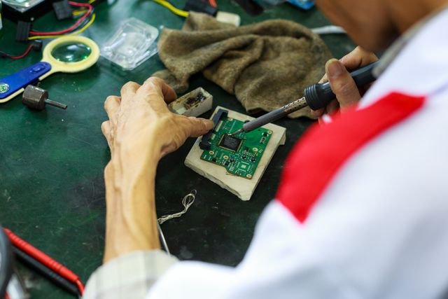
Sending your first PCB design for manufacturing is an exciting step.
It is also the point where small design mistakes become physical problems.
A reversed connector, an incorrect footprint, a missing pull-up resistor, or one unavailable component can delay the entire prototype. Sometimes the issue can be repaired with a wire or a replacement part. In other cases, the only practical solution is to revise the design and order another board.
That does not mean the first version has to be perfect. Prototypes are built to reveal problems and confirm assumptions. However, many expensive prototype failures are not caused by difficult engineering challenges. They happen because basic design, documentation, or assembly checks were missed before the order was placed.
A structured review can prevent most of these avoidable problems.
This prototype PCB assembly checklist covers the key items to verify before releasing your first board for fabrication and assembly. It includes the schematic, PCB layout, component availability, manufacturing files, programming access, mechanical fit, and the testing plan you will need once the boards arrive.
Why the Final Review Matters
A PCB design can look complete on a computer screen while still containing problems that only become visible after assembly.
The schematic may be electrically correct, but the selected component footprint may not match the actual package. The board outline may fit the enclosure, but the USB connector may be positioned too far inside the case. The microcontroller may be wired correctly, but no programming header has been included.
These issues are easy to overlook because PCB design involves several connected layers:
- Electrical design
- Component selection
- PCB layout
- Mechanical integration
- Manufacturing
- Assembly
- Firmware
- Testing
A change in one area can create a problem somewhere else.
For example, replacing a component in the bill of materials may affect the footprint, operating voltage, firmware, or enclosure clearance. A board that passes electrical design checks may still be difficult to assemble or test.
The final review should therefore look at the product as a complete system, not only as a schematic and layout.
1. Confirm That the Requirements Are Still Correct
Before reviewing individual traces or component values, return to the original product requirements.
PCB projects often change during development. Features are added, sensors are replaced, communication methods are updated, and enclosure dimensions shift. The schematic and layout may contain parts from different stages of the project.
Confirm the board still supports the required:
- Input voltage
- Power consumption
- Processor performance
- Memory
- Sensors
- Communication interfaces
- Connectors
- User controls
- Status indicators
- Programming method
- Operating temperature
- Physical dimensions
- Mounting method
It is also worth checking whether any features were included during early development but are no longer needed.
Removing unnecessary components can reduce assembly cost, simplify testing, and free PCB space. However, do not remove useful debugging access simply to make the first prototype look cleaner. Test points, indicator LEDs, and configuration headers often save time during board bring-up.
2. Review the Complete Schematic
The schematic should be reviewed page by page before generating manufacturing files.
Do not only look for obvious wiring errors. Check whether each circuit has everything it needs to operate reliably.
Review:
- Power connections
- Ground connections
- Component values
- Pin numbers
- Signal names
- Interface voltage levels
- Pull-up and pull-down resistors
- Decoupling capacitors
- Protection components
- Connector pinouts
- Reset circuits
- Clock circuits
- Programming connections
It is helpful to review the schematic by function.
For example, inspect the power section separately from the microcontroller, sensors, communication circuits, and output drivers. This makes it easier to think through how each part will operate.
Ask practical questions:
- What happens when power is first applied?
- Is the processor guaranteed to start in a known state?
- Could any output turn on unexpectedly during reset?
- Are floating inputs possible?
- Can one powered section feed voltage into another unpowered section?
- Are external signals protected?
- Are unused pins handled correctly?
A second engineer or designer should review the schematic where possible. The person who created the design often sees what they intended rather than what is actually connected.
3. Run the Electrical Rules Check
Most PCB design tools include an electrical rules check, commonly called ERC.
The ERC can identify issues such as:
- Unconnected pins
- Conflicting output pins
- Missing power flags
- Unpowered components
- Incorrect pin types
- Duplicate references
- Unexpected net connections
Do not simply clear every warning until the list is empty.
Some warnings are harmless, but each one should be understood. If a warning is intentionally ignored, document the reason. This prevents a genuine issue from being hidden among dozens of accepted warnings.
The ERC will not understand the complete design intent. It may not know that two connected devices use incompatible voltage levels or that a resistor value is unsuitable. It is a useful checking tool, not a replacement for engineering review.
4. Verify Power Inputs and Voltage Rails
Power mistakes are among the most damaging PCB prototype errors.
Begin with the external power source.
Confirm:
- Input voltage range
- Maximum current requirement
- Connector polarity
- Reverse-polarity protection
- Fuse or overcurrent protection
- Surge and transient protection
- Power-switch ratings
- Regulator input limits
Then review every internal voltage rail.
Check that:
- Each component uses the correct supply voltage
- Regulator output voltages are correct
- Regulator current capacity is sufficient
- Power dissipation is acceptable
- Required input and output capacitors are present
- Capacitor values and ESR requirements are suitable
- Enable pins are controlled correctly
- Power sequencing is acceptable
A regulator that works at room temperature on a lightly loaded bench may overheat inside an enclosure under full load. Consider both electrical load and thermal conditions.
For switching regulators, confirm the inductor, diode, feedback resistors, compensation network, and layout follow the device manufacturer’s recommendations.
5. Check Decoupling and Bulk Capacitance
Every digital integrated circuit should have appropriate local decoupling.
Decoupling capacitors should normally be placed close to the relevant power pins, with short connections to power and ground.
Verify:
- Every IC has the recommended decoupling capacitors
- High-speed devices have sufficient local capacitance
- Analog supply pins are treated correctly
- Bulk capacitors are available near major loads
- Capacitor voltage ratings provide adequate margin
- Polarized capacitors are oriented correctly
The exact requirements depend on the device.
A microcontroller, radio module, motor driver, and sensor may all require different capacitor arrangements. Follow the component datasheet rather than applying one generic capacitor value everywhere.
6. Verify Component Footprints
A correct schematic symbol does not guarantee a correct PCB footprint.
This is one of the most common causes of failed PCB prototypes.
For every component, verify:
- Package type
- Pin count
- Pin numbering
- Pad dimensions
- Pad spacing
- Exposed thermal pads
- Polarity markings
- Mechanical dimensions
- Recommended land pattern
Pay particular attention to:
- Connectors
- Voltage regulators
- Transistors
- Diodes
- LEDs
- Electrolytic capacitors
- Crystals
- USB connectors
- Fine-pitch ICs
- Similar-looking package variants
A connector footprint may match the electrical pin count but use the wrong mounting orientation. A transistor may be available in several pin configurations under the same package name.
Do not rely only on a library component name. Compare the footprint with the exact manufacturer datasheet and purchasing part number.
For critical parts, print the PCB layout at actual size and place the physical component over the footprint. This simple check can reveal mechanical and orientation problems quickly.
7. Confirm Pin 1 and Component Orientation
Polarity and orientation mistakes can affect the entire assembly batch.
Check orientation for:
- Integrated circuits
- Diodes
- LEDs
- Electrolytic capacitors
- Tantalum capacitors
- Transistors
- Connectors
- Battery holders
- Crystals with numbered pads
Make sure the schematic symbol, PCB footprint, assembly drawing, and silkscreen all use the same orientation.
Pin 1 markings should be visible after assembly where possible.
Avoid placing a tiny orientation mark underneath the component where technicians cannot see it. A clear dot, notch, line, or label can reduce assembly mistakes and simplify inspection.
Connector orientation deserves special attention. Ask whether the cable exits in the expected direction and whether the mating connector can be inserted after the PCB is installed in the enclosure.
8. Review the Bill of Materials
The bill of materials, or BOM, should contain enough information for purchasing and assembly teams to identify every part without guessing.
Each BOM entry should normally include:
- Reference designators
- Quantity
- Component description
- Value
- Package
- Manufacturer
- Manufacturer part number
- Approved alternative where applicable
- Assembly status
- Supplier information where required
Avoid vague entries such as:
- “10k resistor”
- “USB connector”
- “3.3V regulator”
These descriptions may correspond to many different components.
The manufacturer part number is especially important for ICs, connectors, sensors, crystals, and power components.
Also check whether components marked as “do not populate” are clearly identified. The BOM, pick-and-place file, and assembly drawing should all agree about which parts are fitted.
9. Check Component Availability Before Ordering
A technically suitable component is not useful if it cannot be purchased.
Before releasing the design, check:
- Current stock
- Minimum order quantity
- Lead time
- Lifecycle status
- Package availability
- Approved distributors
- Possible alternatives
- Counterfeit risk
- Pricing at prototype and production quantities
Shortages often affect microcontrollers, communication modules, sensors, connectors, and power components.
Replacing an unavailable component after layout completion may require:
- A new footprint
- Different supporting components
- Firmware changes
- Changed power requirements
- New regulatory testing
For first prototypes, using parts already stocked by the assembly provider can simplify purchasing and shorten lead time.
However, do not choose a weak technical component only because it is immediately available. Consider whether the same part or a suitable alternative can support future production.
10. Confirm Voltage-Level Compatibility
Many modern PCB designs use components operating at different voltages.
A microcontroller may use 3.3V logic while a peripheral uses 5V. A sensor output may exceed the processor’s input rating. An external interface may require a level shifter or protection network.
Check every interface for:
- Logic-high and logic-low thresholds
- Maximum input voltage
- Output voltage
- Open-drain requirements
- Pull-up voltage
- Bidirectional communication
- Power-off behaviour
Common interfaces requiring careful review include:
- I²C
- SPI
- UART
- USB
- CAN
- RS-232
- RS-485
- GPIO connections
- External sensor inputs
A circuit may appear to work during a quick test while operating outside the component’s recommended limits. That can lead to unreliable behaviour or long-term damage.
11. Review Connector Pinouts Carefully
Connector errors are easy to make and inconvenient to repair.
Verify every connector against:
- Cable drawings
- Mating connector orientation
- External equipment pinout
- Mechanical keying
- Pin numbering direction
- Ground and power positions
- Current rating
- Voltage rating
Do not assume pin numbering follows the same direction when viewed from the cable side and PCB side.
For external connectors, consider what happens if the cable is inserted incorrectly or connected to the wrong device. Keyed connectors, labels, protection, and different connector types can reduce installation errors.
Place clear silkscreen labels near development and test connectors.
Labels such as GND, 3V3, TX, RX, SWD, and RESET are much more useful than relying only on a reference designator.
12. Run the Design Rules Check
The PCB design rules check, or DRC, should be run using the actual capabilities of the selected manufacturer.
Check:
- Minimum trace width
- Minimum clearance
- Via diameter
- Drill size
- Annular ring
- Copper-to-edge clearance
- Solder-mask clearance
- Silkscreen-to-pad clearance
- Differential pair rules
- Controlled-impedance requirements
Do not use extremely small features unless the design genuinely requires them.
Tighter fabrication rules can increase cost and reduce manufacturing options. A prototype that uses conservative dimensions is often easier to manufacture, inspect, and rework.
Review every DRC warning rather than relying only on the final error count.
13. Check Trace Widths and Current Capacity
Not every signal should use the same trace width.
Power and high-current paths need to be sized according to:
- Expected current
- Copper thickness
- Acceptable temperature rise
- Trace length
- Layer
- Available cooling
Review:
- Input power paths
- Battery connections
- Motor outputs
- Heater connections
- Relay contacts
- High-current ground returns
- Regulator inputs and outputs
Also consider vias in high-current paths.
A wide trace may still be restricted by one small via. Multiple vias or larger plated holes may be required when current moves between layers.
For high-current designs, connector ratings, terminal blocks, fuses, switches, and copper areas must all support the same load.
14. Review Grounding and Return Paths
A signal does not travel only through its visible trace. It also needs a return path.
Poor return-path design can create:
- Noise
- Unstable communication
- Incorrect sensor readings
- Electromagnetic interference
- Radio-performance problems
- Unexpected resets
Check that high-speed signals have a continuous reference plane and do not cross splits in the ground plane.
Keep noisy current paths, such as motor drivers and switching regulators, away from sensitive analog circuits where possible.
For mixed-signal designs, grounding should be planned according to the actual current flow rather than using arbitrary ground splits.
Pay attention to:
- Analog sensor returns
- High-current load returns
- USB and communication grounds
- Shield connections
- Chassis ground
- Battery ground
- Power-supply ground
15. Inspect Critical Signal Routing
Some signals require more careful routing than general GPIO.
Review:
- Clock lines
- Crystal traces
- USB differential pairs
- Ethernet pairs
- High-speed SPI
- Memory buses
- RF paths
- Analog sensor signals
- Switching regulator loops
Crystal components should normally be placed close to the processor, with short and symmetric traces where recommended.
Differential pairs should follow the required spacing, length matching, and impedance rules.
Sensitive analog signals should be kept away from switching nodes, clocks, and high-current traces.
For RF designs, antenna layout and keep-out areas should follow the module or antenna manufacturer’s reference design closely.
16. Check Component Spacing for Assembly
A board can pass DRC and still be difficult to assemble.
Verify there is enough space for:
- Pick-and-place equipment
- Soldering tools
- Inspection
- Rework
- Connector mating
- Test probes
- Heat sinks
- Mechanical fasteners
Avoid placing tall components too close to small parts that may need rework.
Check that component courtyards do not overlap and that assembly tools can reach through-hole pins and connectors.
For hand-assembled prototypes, very small packages can increase difficulty and cost. A 0402 component may fit easily, but an 0603 or 0805 part may be more practical when board space is not critical.
17. Use Consistent Component Orientation
Where possible, orient similar polarized components in the same direction.
For example:
- Place IC pin 1 consistently
- Align diode cathodes
- Align polarized capacitors
- Keep resistor and capacitor text readable in similar directions
Consistent orientation helps assembly and visual inspection.
It also reduces the chance of manual placement mistakes, especially during prototype rework or partial hand assembly.
18. Add Fiducials Where Needed
Fiducials are visual reference marks used by automated assembly equipment to align the PCB.
They may be required for:
- Automated SMT placement
- Fine-pitch components
- Panelized boards
- Larger PCBs
- Double-sided assembly
Your assembly provider may require global board fiducials and local fiducials near fine-pitch devices.
Confirm:
- Fiducial size
- Copper clearance
- Solder-mask opening
- Placement
- Number required
Do not assume the manufacturer will add them automatically.
19. Review Solder-Mask and Paste-Mask Openings
Solder-mask and paste-mask settings affect assembly quality.
Check:
- Solder-mask expansion
- Fine-pitch pad openings
- Thermal-pad paste reduction
- Via tenting
- Exposed copper
- Closely spaced pads
- Paste coverage for large pads
Large exposed thermal pads often need the solder-paste opening divided into smaller sections to reduce component floating and excessive solder.
For fine-pitch ICs, incorrect paste openings can create bridges or insufficient solder joints.
The assembly provider may adjust the stencil, but the design files should still reflect the intended assembly approach.
20. Check Thermal Management
Identify components likely to generate heat.
These may include:
- Voltage regulators
- Motor drivers
- Power transistors
- High-power LEDs
- Processors
- Wireless modules
- Power resistors
Review:
- Copper area
- Thermal vias
- Airflow
- Enclosure temperature
- Heat sinks
- Component spacing
- Maximum junction temperature
A component’s current rating may assume a larger copper area than the layout provides.
Thermal performance should be estimated under worst-case load, not only under typical operation.
For the first prototype, include practical methods to measure temperature during testing.
21. Verify Mechanical Dimensions
Electrical correctness will not help if the board does not fit the product.
Confirm:
- Board outline
- Mounting-hole position
- Hole diameter
- Connector location
- Button location
- Display alignment
- Antenna clearance
- Component height
- Keep-out areas
- Cable bend radius
- Enclosure walls
- Screw-head clearance
Use the latest enclosure or mechanical drawing.
A 3D model of the PCB can help identify collisions, but it is only reliable when component models and heights are accurate.
Where possible, import the PCB into the mechanical CAD assembly and check the complete fit.
For unusual or high-risk mechanical layouts, ordering a bare PCB or low-cost mechanical sample before full assembly may be worthwhile.
22. Check the Board Outline and Fabrication Layer
The PCB manufacturer needs a clear, closed board outline.
Verify:
- Only one final outline exists
- The outline is on the correct layer
- Internal cutouts are defined
- Slots are shown correctly
- Routed areas are documented
- Board dimensions are included
- Edge plating is specified if required
Old or hidden outline shapes can create confusion during fabrication.
View the exported Gerber files rather than assuming the CAD source will be interpreted correctly.
23. Add Useful Test Points
Test points are valuable during prototype bring-up and future production testing.
At minimum, consider access to:
- Ground
- Input power
- Each regulated power rail
- Reset
- Programming signals
- Communication buses
- Important analog signals
- Critical control outputs
Test points should be:
- Clearly labelled
- Large enough for probes
- Accessible after assembly
- Placed away from short-circuit risks
- Included in the test documentation
Do not place all test points underneath large components or close to exposed high-voltage areas.
A few well-positioned test points can save hours of troubleshooting.
24. Confirm Programming and Debug Access
A newly assembled board may be electrically correct but unusable if the processor cannot be programmed.
Verify:
- Programming connector pinout
- Programming voltage
- Ground connection
- Reset connection
- Boot-mode configuration
- Debug signals
- Connector orientation
- Required pull resistors
- Tool compatibility
For microcontrollers, this may involve:
- SWD
- JTAG
- ICSP
- UART bootloader
- USB bootloader
Make sure the programming interface remains accessible after the board is installed in the enclosure, or define a separate production-programming method.
If firmware will be programmed by the assembly provider, supply clear instructions and the correct binary files.
25. Decide What Firmware the Board Needs at Assembly
Some prototypes are assembled without firmware and programmed later. Others require firmware during assembly testing.
Confirm:
- Which firmware version should be used
- File format
- Programming tool
- Memory addresses
- Security settings
- Serial-number handling
- Calibration data
- Verification process
Avoid sending an unlabelled file such as final.bin.
Use clear revision names and keep the firmware release linked to the corresponding PCB revision.
Hardware and firmware should be managed together. A firmware version developed for an earlier PCB may use different pins or peripherals.
26. Prepare a Complete Assembly Drawing
The assembly drawing should show the PCB with reference designators and component outlines.
It may also include:
- Board revision
- Top and bottom views
- Polarity notes
- Special component orientation
- Do-not-populate parts
- Mechanical hardware
- Assembly instructions
- Programming requirements
Make sure the drawing is readable.
Reference designators should not overlap components or become too small to use. Special instructions should not be hidden inside email messages that may be missed by the assembly team.
27. Generate and Review the Pick-and-Place File
The pick-and-place file tells automated equipment where each component is placed and how it is rotated.
It normally includes:
- Reference designator
- X coordinate
- Y coordinate
- Rotation
- Board side
Verify:
- Units
- Origin
- Top and bottom identification
- Rotation values
- Included components
- Excluded components
- Component center positions
Rotation conventions can differ between design tools and assembly providers.
Do not assume the exported orientation is correct simply because the file was generated successfully. Compare several polarized components with the assembly drawing.
28. Generate and Inspect Gerber Files
Gerber files describe the copper, solder mask, silkscreen, paste, and board outline used for fabrication.
Typical files include:
- Top copper
- Bottom copper
- Internal copper layers
- Top solder mask
- Bottom solder mask
- Top silkscreen
- Bottom silkscreen
- Top paste
- Bottom paste
- Board outline
- Drill files
Open the exported files in an independent Gerber viewer.
Inspect:
- Board outline
- Copper layers
- Missing planes
- Text orientation
- Solder-mask openings
- Silkscreen over pads
- Drill alignment
- Slots and cutouts
- Layer order
This step catches export and configuration mistakes that may not appear inside the design tool.
29. Verify Drill Files and Hole Types
Review all drilled features.
Confirm:
- Plated through-holes
- Non-plated holes
- Mounting holes
- Slots
- Via sizes
- Tool sizes
- Connector holes
A mounting hole may need to be non-plated, while a connector pin requires plating. Incorrect hole classification can affect mechanical fit or electrical connection.
Make sure slots are defined in a format the selected manufacturer accepts.
30. Confirm the PCB Stack-Up
For simple two-layer boards, the stack-up may be straightforward. Multilayer and controlled-impedance designs need more attention.
Confirm:
- Layer count
- Copper thickness
- Board thickness
- Dielectric material
- Impedance requirements
- Layer order
- Plane assignments
- Surface finish
If controlled impedance is required, coordinate with the PCB manufacturer before finalising trace widths.
Do not use generic impedance values without considering the manufacturer’s actual stack-up.
31. Select the Appropriate Surface Finish
Common PCB finishes include:
- HASL
- Lead-free HASL
- ENIG
- Immersion silver
- Immersion tin
The best option depends on:
- Component pitch
- Shelf life
- Assembly method
- RoHS requirements
- Cost
- Contact surfaces
- Wire bonding
- RF requirements
ENIG is commonly chosen for fine-pitch prototypes because it provides a flat surface, but it may cost more than HASL.
Discuss special requirements with the manufacturer rather than choosing only by price.
32. Confirm Panelization Requirements
Small boards are often manufactured and assembled in panels.
Ask the supplier whether panelization is required and who will prepare it.
Consider:
- Panel size
- Board spacing
- Tooling rails
- Fiducials
- Breakaway tabs
- V-scoring
- Mouse bites
- Component distance from edges
- Depanelization method
Components placed too close to a breakaway edge may experience mechanical stress during depanelization.
For early prototypes, the assembly provider may handle panelization. Confirm this before sending files.
33. Define Acceptable Component Substitutions
Assembly providers may suggest alternative resistors, capacitors, or other parts when the specified item is unavailable.
Some substitutions are low risk. Others can affect performance significantly.
Define whether substitutions are allowed for:
- Passive components
- Regulators
- Crystals
- Sensors
- Connectors
- Memory
- Microcontrollers
- Wireless modules
For every approved alternative, verify:
- Electrical rating
- Tolerance
- Temperature coefficient
- Package
- pinout
- frequency characteristics
- lifecycle
- firmware compatibility
Do not allow important components to be substituted without engineering approval.
34. Decide How the First Boards Will Be Tested
The testing plan should exist before the boards arrive.
A basic first-board plan may include:
- Visual inspection
- Resistance check between power and ground
- Continuity checks
- Current-limited power-up
- Voltage-rail verification
- Clock and reset checks
- Processor programming
- Communication-interface testing
- Sensor and output testing
- Thermal inspection
- Functional testing
Prepare:
- Test equipment
- Firmware
- Cables
- Programming tools
- Mating connectors
- Power supplies
- Loads
- Expected measurements
Without a plan, teams often power the board immediately and begin debugging several unknowns at once.
35. Plan for Current-Limited First Power-Up
The first power-up should normally use a bench supply with a safe current limit.
Before applying power:
- Inspect for solder bridges
- Confirm component orientation
- Check resistance between power and ground
- Verify input polarity
- Remove unnecessary external devices
- Set the correct voltage
- Set a conservative current limit
Monitor the board for:
- Unexpected current draw
- Heating
- Smoke or smell
- Incorrect voltage rails
- Repeated resets
Do not begin by connecting the prototype directly to a high-current battery or unrestricted power adapter.
36. Order a Sensible Prototype Quantity
There is little value in assembling a large batch before the design has been tested.
The right prototype quantity depends on:
- Project complexity
- Assembly setup cost
- Destructive testing needs
- Firmware development
- Multiple engineering teams
- Customer demonstrations
- Regulatory testing
- Expected rework
A small initial quantity reduces risk, but ordering only one board can also be inconvenient.
The single board may be damaged during testing, and several engineers may need access at the same time.
For many projects, a small batch allows one board for bring-up, one for firmware development, one for mechanical testing, and additional units for backup or comparison.
37. Use Clear Revision Control
Every PCB prototype should have a clear revision identifier.
Include the revision on:
- PCB silkscreen
- Schematic
- Layout file
- BOM
- Gerber package
- Assembly drawing
- Firmware release
- Test report
Avoid unclear names such as:
- final
- final2
- newfinal
- latest
Use a consistent structure such as:
- Hardware Revision A
- Hardware Revision B
- Prototype 1.0
- Prototype 1.1
Keep a record of what changed between revisions.
This becomes essential when several board versions are being tested at the same time.
38. Package the Manufacturing Files Clearly
Before sending the project, create one controlled release package.
It may contain:
- Gerber files
- Drill files
- BOM
- Pick-and-place file
- Assembly drawings
- Fabrication drawing
- Stack-up information
- Special instructions
- Firmware
- Programming instructions
- Test requirements
- Readme document
Remove old exports and unused drafts from the package.
The manufacturer should not have to decide which file is current.
The readme document can list:
- Project name
- PCB revision
- Quantity
- Layer count
- Board thickness
- Copper thickness
- Surface finish
- Assembly sides
- Special components
- Substitution rules
- Contact information
39. Ask the Manufacturer for a File Review
Many PCB fabrication and assembly providers offer a manufacturing review before production.
They may identify:
- Missing files
- Unavailable components
- Footprint concerns
- Panelization issues
- Solder-mask problems
- Assembly clearances
- Incorrect rotations
- Fabrication-rule violations
A manufacturer review is valuable, but it does not replace your own design verification.
The supplier checks whether the board can be manufactured and assembled. They may not know whether the circuit will perform the intended function.
40. Review the Assembly Confirmation Carefully
Before assembly begins, the provider may send:
- Component availability report
- Substitution list
- Placement drawing
- Production file confirmation
- Questions about orientation
- Updated quotation
Do not approve these documents without reviewing them.
Confirm that:
- All expected parts are included
- No critical parts were substituted incorrectly
- Do-not-populate parts remain unassembled
- Component orientation is correct
- The board revision is correct
- The quantity is correct
- Programming and testing instructions are included
A quick approval at this stage can allow an avoidable mistake to reach every board in the batch.
Common Prototype PCB Assembly Mistakes
Using an Unverified Footprint
The symbol is correct, but the physical package does not match the footprint.
Reversing a Connector
The pin numbers are interpreted from the wrong viewing direction.
Missing Programming Access
The processor is assembled correctly, but no usable programming connection exists.
Forgetting Test Points
Basic voltage and communication signals cannot be reached safely during debugging.
Ordering Before Checking Stock
A key component is unavailable, forcing a redesign or long delay.
Using Incorrect Component Rotation
The pick-and-place file does not match the assembly drawing.
Ignoring Mechanical Fit
The board works electrically but does not align with the enclosure.
Weak Power Review
The regulator overheats, the input polarity is wrong, or the power supply cannot support peak current.
Too Much Confidence in Automated Checks
ERC and DRC pass, but the design still contains functional or mechanical errors.
No Structured Bring-Up Plan
The board is powered immediately without checking for shorts, current draw, or voltage rails.
A Compact Pre-Order Checklist
Before approving prototype PCB assembly, confirm that:
- The product requirements are current
- The schematic has been reviewed
- ERC and DRC results are understood
- Power rails and current requirements are correct
- Component footprints match exact part numbers
- Polarized parts have clear orientation
- The BOM is complete
- Components are available
- Logic levels are compatible
- Connectors use the correct pinout
- Trace widths support the expected current
- Ground and return paths are appropriate
- Critical signals are routed correctly
- Components have sufficient assembly clearance
- Fiducials are included where required
- Thermal management has been reviewed
- The PCB fits the mechanical design
- Test points are accessible
- Programming access is available
- Gerbers and drill files have been independently inspected
- Pick-and-place data has been reviewed
- Assembly drawings are clear
- Firmware and programming instructions are ready
- A first-power-up plan exists
- Revision names are consistent
- The manufacturing package contains only approved files
How DevoForge Supports PCB Design and Assembly
At DevoForge, we support hardware projects from early concept development through prototype PCB assembly and preparation for production.
Our PCB design and assembly services can include:
- Requirements review
- Component selection
- Schematic design
- PCB layout
- Power and signal-integrity review
- Design for manufacturing
- Design for assembly
- BOM preparation
- Gerber and production-file generation
- Prototype assembly coordination
- Firmware development
- Board bring-up
- Functional testing
- Design revision
- Low-volume production preparation
- Manufacturing support
We look beyond the board layout itself.
The PCB must work with the firmware, sensors, enclosure, power source, communication system, and final manufacturing process.
The objective is not simply to deliver fabrication files. It is to help turn the design into a working and testable hardware product.
Frequently Asked Questions
What files are needed for prototype PCB assembly?
Most assembly providers require Gerber files, drill files, a bill of materials, a pick-and-place file, and assembly drawings. Additional programming or testing instructions may also be needed.
How many PCB prototypes should I order?
The right quantity depends on development, testing, setup costs, and project risk. Ordering several boards is often more practical than ordering only one.
Should I assemble the first PCB by hand?
Hand assembly may be suitable for simple boards with larger components. Automated SMT assembly is generally better for fine-pitch devices, BGAs, small packages, or repeatable multi-board builds.
What is the most common PCB prototype mistake?
Incorrect footprints and component orientation are among the most common problems. Power and connector mistakes are also frequent.
Do I need test points on a prototype PCB?
Yes. Test points for power rails, ground, programming, and critical signals can make troubleshooting significantly easier.
Should I check component stock before finishing the PCB layout?
Yes. Availability should be checked before the final layout because replacing a component may require changes to the footprint, circuitry, or firmware.
What is the difference between PCB fabrication and assembly?
Fabrication produces the bare PCB. Assembly places and solders electronic components onto the board.
What is design for assembly?
Design for assembly means arranging components, footprints, spacing, orientation, and documentation so the board can be assembled reliably and efficiently.
Can the assembly provider verify my PCB design?
The provider may identify manufacturing and assembly issues, but they may not verify the complete electrical function. Engineering design review remains your responsibility.
What should I test first when the assembled PCB arrives?
Begin with visual inspection, short-circuit checks, and current-limited power-up. Verify power rails before programming the processor or connecting external equipment.
Can PCB assembly companies program firmware?
Many assembly providers offer programming services. They will need the correct firmware, programming procedure, hardware interface, and verification requirements.
When should a prototype move to production?
A board should move toward production after electrical, firmware, mechanical, thermal, reliability, and user requirements have been validated. The design should also undergo DFM, DFA, and production-test review.
Final Thoughts
The purpose of a first PCB prototype is to answer questions.
Does the circuit work? Does the firmware communicate with the hardware? Does the board fit the enclosure? Can the design be assembled and tested reliably?
A prototype does not need to be the final production design, but it should be prepared carefully enough to provide useful answers.
Reviewing the schematic, footprints, BOM, manufacturing files, test access, and mechanical layout before ordering can prevent delays that have little to do with the real engineering challenge.
The best prototype PCB assembly projects begin with clear files, verified components, realistic testing plans, and controlled revision management.
That preparation makes the first board easier to assemble, safer to power, and much faster to debug.
Preparing to order your first PCB prototypes? Speak with the DevoForge engineering team about your schematic, layout, assembly files, firmware, and board-testing requirements.